Abstract
This paper describes how silicon photonic (SiPh) opto-electronic integration and packaging, with its improved RF performance, is designed to: (1) enable next-generation coherent transmission beyond 100Gbaud; and (2) provide network operators with the ability to avoid “half-step” capacity upgrades and allow them the full step upgrades they need without sacrificing reach or stranding network bandwidth when migrating from current-generation solutions.
Introduction
Similar to consumer electronic devices, high-capacity optical transceiver modules have followed a path towards size reduction with increased performance and functionality. This has been driven by growing bandwidth demands in data center and service provider networks as a result of applications such as cloud services, content streaming, and social media. To meet these growing demands, network operators are seeking high-performance, high-density and low-power coherent optical interconnect solutions. Coherent optics suppliers are responding with large-scale investments and advancements in silicon photonic (SiPh) opto-electronic integration and packaging to introduce compact, high-performance, volume-manufacturable designs that can enable them to meet this growing demand.
Advancements in coherent optics are important for network operators to efficiently evolve their networks as bandwidth demand continues to grow. However, as the gap to Shannon’s Limit (the theoretical limit of channel capacity) decreases, it is becoming more difficult to increase capacity and reduce cost per bit by primarily focusing on increasing the modulation order. Beyond the coherent modulation order of 64QAM, fewer transport applications can be supported due to the resulting reduction of achievable link distances, which leaves higher baud rates and advances in packaging technology as preferred ways to increase capacity and decrease cost per bit. As a result, industry investments are shifting toward increasing the transmission aggregate baud rate to increase capacity while maintaining usable reaches. A direct benefit of these investments and advancements includes electrical high-frequency radio frequency (RF) performance improvements inside the module.
This paper describes how SiPh opto-electronic integration and packaging, with its improved RF performance, is designed to: (1) enable next-generation coherent transmission beyond 100Gbaud; and (2) provide network operators with the ability to avoid “half-step” capacity upgrades and allow them the full step upgrades they need without sacrificing reach or stranding network bandwidth when migrating from current-generation solutions.
Higher Baud Rates for Smooth Network Evolution
The requirements for higher baud rates of optical transceivers to increase the transmission distance and to reduce the cost-per-transmitted bit in turn drives the need for wider optical channels, i.e., wider pass bands or channel spacing. Due to long upgrade intervals as a result of high CapEx and OpEx, careful consideration must be taken in the channel/passband requirements for next-generation optical line system deployments. Even though today’s reconfigurable optical add-drop multiplexers (ROADMs) can support a flexible range of channel widths, network operators often find that adhering to standard intervals of channel widths is a preferable option. This enables them to utilize channel spacing based on regular multiples that can be combined without stranding spectrum due to fragmentation1. Earlier generations of dense wavelength division multiplexing networks have deployed 50, 75, and 100GHz channels.
To accommodate future transmission schemes while minimizing stranded bandwidth using half-step upgrades, network operators may seek to ensure wider channel plans are integer multiples of recently established plans, such as two times 75GHz as illustrated in Figure 1.

Figure 1. Channel plan evolution to accommodate coherent transmission trends; migrating to wider channels enables scalability.
150GHz-wide channels are now seen as the next evolutionary step for future-proofing the line system for higher-capacity network architectures, doubling the channel bandwidth (thereby accommodating a doubling of baud rate) of current 75GHz implementations. A wide-channel-capable line system can also provide the network operator with the ability to accommodate multiple coherent transmission techniques.
By dialing down the modulation order and doubling the baud rate, solutions can expand current capacities over a much greater distance. A 150GHz channel plan can accommodate these higher aggregate baud rates. Avoiding intermediate steps of baud rate increases can remedy the issue of stranded bandwidth when a 150GHz channel plan is used1. In addition to minimizing stranded bandwidth, a wide 150GHz channel also allows for higher capacity per transponder which in turn reduces the cost-per-bit as well as the number of channels required to maximize fiber capacity. This can lower operational cost/complexity and result in a reduction in required ROADM ports.
Current coherent transmission solutions operate in the range of 60Gbaud through 70Gbaud, and doubling the rate obviously also introduces a range to more efficiently utilize a 150GHz channel. For brevity, in the remainder of this article we refer to this doubling range as greater-than 100Gbaud. It is also important to emphasize that baud rates below 100Gbaud do not fully utilize a 150GHz channel passband.
High-speed modulators and RF interconnects for next-gen optics

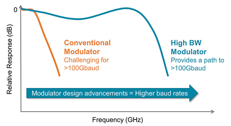
Figure 2 illustrates how high bandwidth SiPh optical modulator designs can support >100Gbaud coherent transmission capabilities to efficiently fill 150GHz channel width line-system architectures.

Figure 2. Illustration of simulated frequency response of a high-bandwidth SiPh optical modulator capable of supporting >100Gbaud coherent transmission speeds.
Even with an optical modulator having ample frequency response to support >100Gbaud transmission, there is another key factor that could limit the optical transmission speed. The electrical interconnects of the PIC and surrounding RF components such as electrical drivers can become a limiting factor in transmission performance and design complexity. Additionally, the RF performance at these speeds is sensitive to impairments along the electrical path between the coherent digital signal processor (DSP) and the PIC as well as its surrounding RF components. In traditional designs (Figure 3), the high-speed RF electrical signal may traverse between these components over multiple physical interfaces such as solder ball-grid array (BGA) bumps/balls, substrate, printed circuit board traces, wire bonds, and gold-box lead-frame pins, with each element introducing parasitics and losses that degrade signal integrity. This applies to next-generation optical solutions in general, regardless of whether the transmission technique is coherent or not. Fortunately, techniques to mitigate opto-electronic RF signal impairments already exist in the electronics industry.

Figure 3. Illustration of a conventional high-speed RF electrical interconnect between coherent DSP and PIC.
Opto-electronic RF interconnect evolution for higher speeds
An advantage of SiPh is its ability to leverage mature, volume-manufacturable processes from the electronics industry, such as component stacking (Figure 4). In component stacking, electrical impairments are reduced due to direct electrical connections between key RF components, creating a robust signal path for extremely high frequency/baud rate operation. In this co-packaged/stacked design, the gold-box packaging is eliminated, the DSP and PIC are tightly co-packaged, and the high-speed Si modulator driver and TIA components are stacked on the PIC.

Figure 4. Illustration of a component stacking configuration
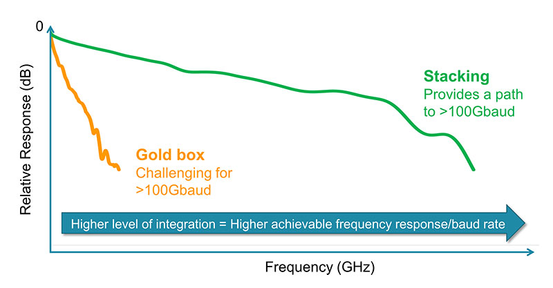
Figure 5 shows the stacked design has a higher (better) frequency response than the traditional gold-box design. Advanced stacking designs to further eliminate interconnect impairments can result in pushing the frequency response even higher.

Figure 5. Illustration of example electrical interconnect frequency response comparing traditional gold-box and stacking integration.
It is noteworthy to mention that the conversion of the analog RF high-speed signals into digital signals for coherent DSP processing are performed by high-speed, high-resolution digital-to-analog convertors (DACs) and analog-to-digital convertors (ADCs). These Si-based devices are able to support >100Gbaud operation, especially when utilizing next generation CMOS node sizes such as 5nm material and are therefore not a limiting element at these speeds.
Architectural comparisons of SiPh and InP
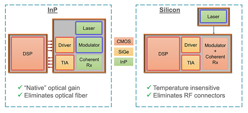
As previously stated, coherent optics designs are generally based on either InP or Si. InP is a direct bandgap semiconductor material well suited for use in optical components such as lasers and modulators. Using InP, these functions can be fabricated on the same chip (see figure 6). In contrast, Si is an indirect-bandgap semiconductor material, commonly used to fabricate various electronic components including DSPs and other ASICs. Si is also used to fabricate SiPh devices such as modulators and coherent receivers. However, silicon does not allow for the straightforward fabrication of lasers. As a result, in a SiPh coherent design, the laser is typically separate from the SiPh PIC and made from a different material such as InP. This separation can be an advantage in thermally challenging environments because the temperature-sensitive InP laser can be designed to be further away from heat-producing ASICs, while the temperature insensitive silicon photonics can be placed closer to the DSP. The co-packaging of the Si/SiPh components enable efficient heat dissipation designs, which can lower overall power consumption. Although the InP laser needs to be located separately, the optical connection is easily achieved using well-known design and manufacturing processes.

Figure 6. Comparison of InP-based and Si-based coherent elements that require high-speed RF electrical interconnects. Red outlined boxes have greater thermal tolerance compared to blue outlined boxes.
Co-packaging of all the Si/SiPh components, as shown in Figure 4, allows stacked high-speed electrical paths that provide high-performance RF interconnects, compared to an InP-based design that may further separate components due to material or thermal mismatches and hermeticity requirements. As previously mentioned, SiPh leverages high-volume manufacturing processes already established in the electronics industry. Acacia’s 3D Siliconization is an example of leveraging these processes to manufacture compact, coherent modules with high-performance electrical RF interconnects. The 3D Siliconization approach takes advantage of mature silicon photonics technology, in-house expertise, and vertical integration, while utilizing high-volume electronics manufacturing processes.
Evolving Networks for Future Growth
Next generation coherent interconnects are designed to offer network operators the ability to evolve their networks to meet growing bandwidth demands. Since this must be done without sacrificing reach or stranding network bandwidth when migrating from current-generation solutions, coherent suppliers have been focusing on increasing the transmission aggregate baud rate to increase capacity while maintaining usable reaches. They have been able to achieve this through continued advancements in SiPh opto-electronic integration and packaging, which has proven to deliver more compact, high-performance, and volume-manufacturable designs.
In the future, SiPh opto-electronic integration and packaging can continue to be important for developing the increased performance and functionality needed for data centers and service providers to meet growing bandwidth demands. Instead of taking half a step to upgrade their network, these advancements can enable them to take the full step with a new generation of coherent optics designed to run beyond 100Gbaud.
References
1 Acacia Communications (2020), “How to Build a Lasting Optical Network,” Retrieved from: https://acacia-inc.com/blog/how-to-build-a-lasting-optical-network/
