Christopher R. Doerr
Acacia Communications, 1301 Route 36, Hazlet, NJ, USA 07730
Abstract. A photonic integrated circuit (PIC) involves a collection of devices on a single substrate that work together to create, guide, mold, or terminate optical photons. Its distant cousin is a high-speed electrical analog (not digital) circuit. PICs find their highest value when integrating many optical components. The technology is finally here to integrate hundreds of optical components together with high yield.
1. Introduction

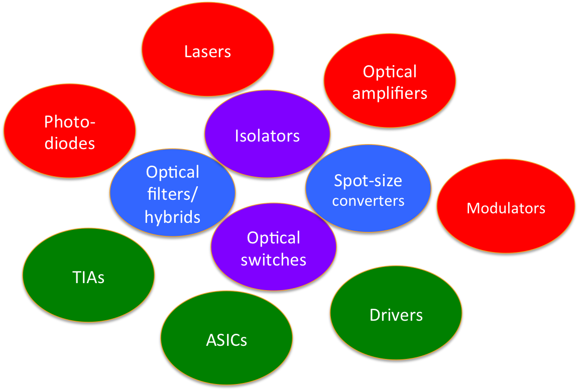
Figure 1. PIC integration candidates. Red is active, blue is passive, green is electronic, and purple is a mix.
According to the dictionary, monolithic is “formed or composed of material without joints or seams”. For an integrated optical circuit, monolithic integration provides lower final cost due to less assembly and less testing, smaller size, higher reliability, and even enhanced performance. In the past, the success of monolithic integration was limited by low yields of the individual components and significant performance trade-offs. Today, tremendous progress has been made and monolithic integrated optical circuits with hundreds of components and actually performance enhancements are a commercial reality [1].
There is a myriad of somewhat conflicting terminology for integrated optical circuits. Optical components are categorized into “active” and “passive”. There is a large range of what is considered to be an active optical component. At one end of the range is devices with only optical gain and the other is devices with any dynamic or electronic behavior. Here we will use the term “active” for any optical component that involves a dynamic interaction between light and matter. Such interaction types include amplifying, electrooptic, thermooptic, acousto-optic, mechanical, piezoelectric, and liquid-crystal-based. For the overall optical circuit, we will use the following terminology: planar lightwave circuit (PLC) for optical integrated devices that are fully passive (except we will allow thermooptic components), and photonic integrated circuit (PIC) for all other optical integrated devices.
On PICs there are many components that can be integrated, as shown in Fig. 1. They are spot-size converters, switches, couplers, isolators, filters, lasers, modulators, optical amplifiers, electronic applicationspecific integrated circuits (ASICs), transimpedance amplifiers (TIAs), photodiodes, modulators, and drivers. Undoubtedly more will develop in the future, such as multimode fiber couplers, thermoelectric coolers, and beam steerers.
2. Material systems
We will focus on semiconductor PICs, because they have the widest range of integrable materials. The two most popular semiconductor optical integration material platforms are the Group III-V materials and the Group IV materials.

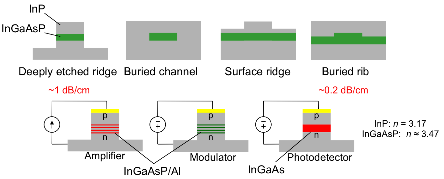
Figure 2. The Group III-V InP family of integrated optic materials.
Typical waveguides made in Group III-V materials are shown in Fig. 2. A rich diversity of structures in the low-loss wavelength regime for fiber-optic transmission (∼1.3-1.6µm) is feasible due to the ability to form lattice-matched ternary and quaternary compounds of InGaAsP as well as substitute Al for P to form InAlGaAs for high-temperature components. Waveguide types range from buried channels to deep ridges.
The primary advantage of the Group III-V platform is that simply by changing the band gap of the materials via composition one can make efficient optical amplifiers, modulators, and photodetectors all in the same platform.

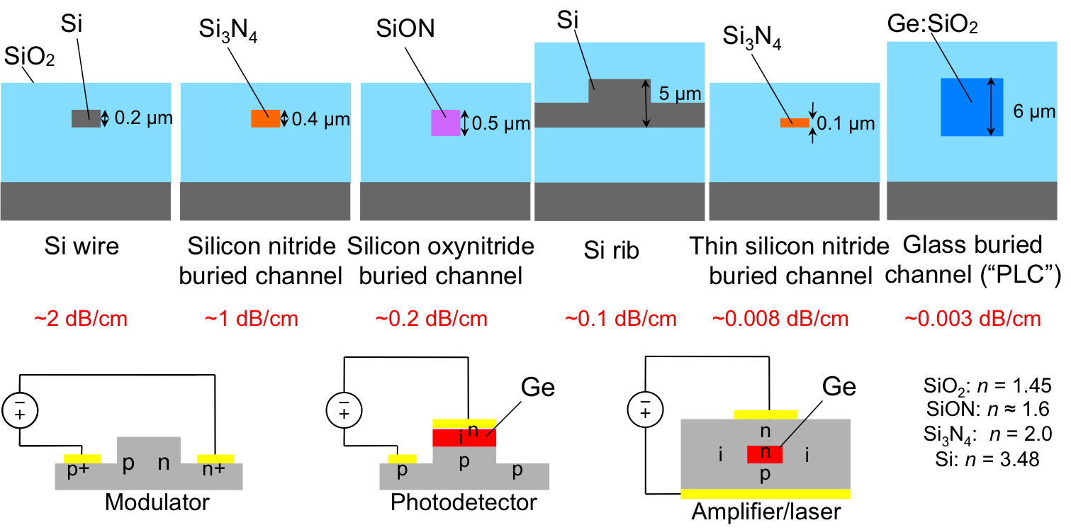
Figure 3. The Group IV family of integrated optic materials.
A non-exhaustive display of the Group IV family of materials is shown in Fig. 3. It invariably involves a Si substrate. On that Si substrate there can be SiO2 (silicon dioxide, often referred to as just oxide), more Si, Si3N4 (silicon nitride), SiON (silicon oxynitride), Ge, and various metals such as Al, Cu, and W. For the Si, there can be crystalline Si (c-Si), amorphous Si (a-Si), and polycrystalline Si (p-Si). The refractive indices of Ge, a-Si, p-Si, c-Si, Si3N4, SiON, and SiO2 at 1550-nm wavelength are approximately 4.2, 3.8, 3.5, 3.48, 2.0, 1.5-1.6, and 1.45, respectively.
The primary advantages of the Group IV material system are the abundance of Si, the high mechanical strength of Si, and Si’s high-quality oxide SiO2. Si makes up 27% of the mass of the Earth’s crust. Ge makes up only 1.4 ppm of the Earth’s crust, but the amount of Ge used in Si PICs is small. Si is very strong mechanically. This allows for potentially high yield and high reliability. It allows for large wafers, the industry currently focusing on 300-mm-diameter wafers for EICs. PICs tend to use previous-generation EIC technology, 200-mm-diameter wafers. Finally, Si has a high quality oxide, SiO2, that is easy to make: when Si is put in an oxygen or steam-rich atmosphere at a high temperature the Si at the surface turns into a high quality, dense oxide. Oxidized Si has extremely low optical loss and is an excellent electrical insulator. For instance, a very small core waveguide of Si3N4 embedded in SiO2 on a Si wafer, in which most of the light resides in the oxide cladding, achieved a waveguide loss of 0.003 dB/cm [2]. The oxide can be molecularly bonded to another wafer also with an oxide layer. Thus nearly all the waveguides in a Group IV PIC are made without epitaxy, allowing for very high PIC yields. The oxide furthermore allows Si optical waveguides to have high index contrast both vertically and horizontally, whereas Group III-V waveguides are generally limited to horizontal high index contrast. High vertical index contrast in InP waveguides has been achieved by using bonded [3] or suspended structures [4], but these are in early research stages. High index contrast in both dimensions allows for very small bend radii (< 5µm) and very strong gratings (making grating couplers possible).
3. Conclusions
We gave some background on optical integration. In the tutorial we will discuss many concrete examples of where PICs really are, both in research and commerce. For some reason, PICs are often thought of having performance trade-offs that preclude use in metro and long-haul applications. We will show that technology has advanced to the point where PICs can now outperform their discrete counterparts. We will also discuss where PICs might be headed next, focusing on what is practical.
Acknowledgements
The author thanks his colleagues at Acacia Communications and Alcatel-Lucent Bell Labs, including L. Chen, D. Vermeulen, B. Mikkelsen, C. Rasmussen, M. Givehchi, L. Zhang, P. J. Winzer, and Y.-K. Chen.
References
- R. Nagarajan, C. Doerr, and F. Kish, “Semiconductor Photonic Integrated Circuit Transmitters and Receivers,” in Optical Fiber Telecommunications VI, 2013.
- J.F. Bauters, M.J.R. Heck, D. John, M.C. Tien, A. Leinse, R.G. Heideman, D. Blumenthal, and J.E. Bowers, “Ultralow loss silica-based waveguides with millimeter bend radius,” 36th European Conference and Exhibition on Optical Communication, pp.1–3, Sept. 2010.
- F. Bordas, G. Roelkens, and R. Zhang, “Compact passive devices in InP membrane on silicon,” ECOC, pp.3–4, 2009.
- L. Chen, L. Zhang, C.R. Doerr, N. Dupuis, N.G. Weimann, and R.F. Kopf, “Efficient Membrane Grating Couplers on InP,” IEEE Photon. Tech. Lett., vol.22, no.12, pp.890–892, 2010.
