C. Doerr, J. Heanue*, L. Chen, R. Aroca, S. Azemati*, G. Ali*, G. McBrien*, Li Chen, B.Guan, H. Zhang, X. Zhang, T. Nielsen, H. Mezghani*, M. Mihnev, C. Yung, and M. Xu
Acacia Communications, Bell Works, 101 Crawfords Corner Road, Holmdel, NJ 07733, USA
*Acacia Communications, 3 Mill and Main Place, Suite 400, Maynard, MA 01754, USA
Abstract: We demonstrate a silicon photonics coherent transceiver in a ball-grid-array
package. It can be handled like a conventional surface-mount-technology component, surviving pick-and-place and 260◦C reflow. It saves cost, size and provides enhanced thermals and bandwidth.
OCIS codes: (060.2330) Fiber optics communications (130.3120) Integrated optics devices.
1. Introduction
An optical coherent system uses the beating between a local oscillator laser and the received signal in order to detect the real and imaginary part of the received optical field. This allows modulation formats that utilize both amplitude and phase, electronic wavelength and polarization demultiplexing, and electronic equalization. This in turn allows for high spectral efficiency and high bit rate per optical carrier, resulting ultimately in the lowest possible cost per bit.
Coherent optics require advanced modulation format modulators, optical hybrids, high-speed photodiodes, polarization combining and splitting optics, variable optical attenuators, and optical monitors for complex control. This large number of optical components benefits greatly from optical integration. However, optical integration provides limited benefit if the packaging dominates the cost of the transceiver.
To date, coherent optics have been put in traditional optical packages: hermetically sealed “gold” boxes. These boxes are made of high-temperature co-fired ceramic (HTCC) with complex features to give a hermetic seal, adding significant cost. Because of the large coefficient of thermal expansion (CTE) mismatch between typical HTCC (∼7 ppm/◦C) and printed circuit board (PCB) material (14 ppm/◦C), the package must use pins or flex cable, which are usually hand-soldered, again increasing cost. Such connections are difficult to get working reliably above ∼30 GHz.
Because of the high temperature firing, HTCC can use only tungsten traces. These traces are lossy at radio frequencies (RF), further limiting bandwidth. Also, gold-box packages normally use wire-bonded components inside. Wire bonds add inductance and variability, further impeding very high-speed performance. Finally gold boxes consume significant PCB real-estate, having protruding, one-dimensional pins and requiring long, meandering RF fanouts on the PCB to match the ASIC or connector.
On the other hand, most high-speed electronic chips today are packaged in ball-grid array (BGA) packages. The die is flip-chip bonded to a substrate. The substrate is made of organic or low-temperature co-fired ceramic (LTCC) and is much lower cost (∼ 10×) than a hermetic HTCC package. The BGA substrate also supports higher bandwidth, using metals with much lower RF losses: copper and gold. BGA packages also have excellent heat sinking, because the backside of the die is connected directly to the lid. BGA packages also support a large number of electrical connections.
The major challenge with an electronic BGA (E-BGA) package is the coefficient of thermal expansion (CTE) mismatch. Unlike a gold box which has bendable pins or a flex cable, there is no mechanical strain relief to take up the significant stress due to CTE mismatch between the PCB (14 ppm/C) and silicon (2.7 ppm/C) in a BGA package. Even worse, the BGA assembly, including the fiber pigtail, must survive a reflow temperature of 260◦C. The BGA is made to work by choosing a substrate material with a relatively high CTE, approaching that of the PCB, to minimize stress on the solder balls. This leaves a large stress between the silicon die and the substrate, which is addressed by using underfill.
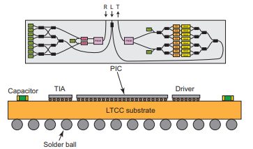
With silicon photonic integrated circuits (PICs) [1], one can use the same BGA technology as for silicon electronic circuits. A coherent transceiver opto-electronic BGA (OE-BGA) schematic is shown in Fig. 1. It contains a silicon PIC (that contains the modulators and receivers), a quad-driver, two dual transimpedance amplifiers (TIAs), and supporting passives such as capacitors. In addition to the CTE-mismatch challenge of an E-BGA, the OE-BGA has an optical fiber connection. A fiber connection to a BGA package is difficult for four main reasons: 1) it must co-exist with underfill, 2) it must be able to be handled by a high-speed pick-and-place machine, 3) it must survive reflow temperature, 260◦C for a few minutes at least three times (PCB top side, PCB bottom side, and rework), and 4) it must survive damp heat.
There has been some published work on silicon-photonic BGA packages [2, 3], but they used right-side up die with wire bonds, which results in a bandwidth limitation due to the long wire-bond step-down and poor heat sinking due to the poor thermal conductivity of the substrate; and reflow and reliability issues were not addressed.

Fig. 1: Schematic of the OE-BGA assembly.
2. Device
Our OE-BGA coherent transceiver consists of an 11-layer LTCC substrate on which were flip-chip bonded a silicon PIC, a quad driver, and two dual TIAs. The package is 21.6mm × 13.0mm, and there are 369 balls. The height is 3.5mm, including the lid. The PIC contains all the optics necessary for a coherent transceiver except the laser, and is similar to that described in [4]. It employs carrier depletion modulators [5] and Ge photodiodes [6]. The transmitter and receiver RF connections are routed inside the BGA substrate to the substrate edge with equal path lengths so that they align directly with the digital-to-analog (DAC) and analog-to-digital (ADC) connections from the ASIC. This is a significantly lower RF loss and more compact way than doing such routing on the PCB.
Before bonding the die, the passives (capacitors, resistors, etc.) were soldered to the BGA using a standard automated PCB assembly surface-mount technology (SMT) line. The die were flip-chip bonded to the substrate, and underfill was applied. Then the SnAgCu solder balls were attached. A photo of the assembled device before fiber attach is shown in Fig. 2(a). The 3-fiber fiber array was attached using an epoxy capable of withstanding 260◦C. A photo of the underside, showing the fiber array and balls, is shown in Fig. 2b. An aluminum lid was attached to the substrate with low-stress epoxy, thermal interface material (TIM) being placed between the backsides of the die and the lid. For one of the BGA assemblies, the fiber pigtail was appropriately protected, and the BGA assembly was placed in a SMT machine. The BGA assembly was automatically placed by the pick-and-place machine and reflowed onto a PCB, as shown in 2(c). An X-ray photo after reflow shows the soldered connections. This shows that an OE BGA can be handled like a conventional E-BGA.

Fig. 2: (a) Substrate and die before fiber attach, (b) Underside, after fiber attach, (c) Reflowed onto PCB, (d) X-ray image of the solder balls.
3. Results
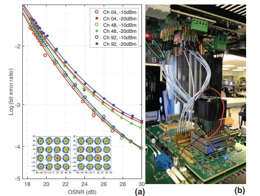
One of the BGA packages was placed in a socket (before soldering it to a PCB) and connected to one core of a dualcore 400-Gb/s coherent ASIC by cables, as shown in Fig. 3(b). The power dissipation in the assembly is 4.9W. The heat-sinking of the BGA is highly effective, the driver die experiencing a temperature rise of only 15 and 8.5◦C over that of the lid and substrate, respectively.
In an optical loopback configuration, the bit-error rate (BER) vs. optical signal-to-noise ratio (OSNR) was measured for non-differential, 30-Gbaud 16-QAM at received signal powers of -10 and -20 dBm at three different wavelengths across the C-band, as shown in Fig. 3(a). 200-Gb/s was successfully transmitted.

Fig. 3: (a) 200-Gb/s 16-QAM real-time BER vs OSNR (0.1-nm bandwidth) for three wavelengths and two different Rx powers. (b) Experimental
setup. The inset in (a) shows the constellation
Three assemblies were taken through a 260◦C 10-minute cycle. The mean optical coupling power change after this solder reflow was < 0.15 dB, and the mean shear strength of the fiber-to-PIC connection was 1.8 kg. The fiber assembly connection to the PIC, on a different substrate, was tested for 500 hours of 85/85 damp heat, and the mean optical coupling power change was < 0.1 dB. Extensive damp heat testing of the BGA package is underway.
In conclusion, we presented an OE-BGA silicon photonics coherent transceiver and demonstrated 200-Gb/s performance. This is a step toward co-packaging of the ASIC and PIC, which will further reduce cost and size and increase RF connection bandwidth. We thank our colleagues at Acacia Communications, including B. Mikkelsen, M. Givhechi, C. Rasmussen, B. Shah, S. Stulz, N. Sauer, A. Cruz, X.-H. Yuan, and R. Manlick for their valuable support of this project.
References
- R. Soref, “The Past, Present, and Future of Silicon Photonics,” IEEE J. Sel. Top. Quantum Electron., vol. 12, no. 6, pp. 1678–1687, 2006.
- H. Tanobe, Y. Kurata, Y. Nakanishi, H. Fukuyama, M. Itoh, and E. Yoshida, “Compact 100Gb/s DP-QPSK integrated receiver module employing three-dimensional assembly technology,” Opt. Express, vol. 22, no. 5, pp. 6108–6113, 2014.
- D. Celo, D. J. Goodwill, J. Jiang, P. Dumais, C. Zhang, F. Zhao, X. Tu, C. Zhang, S. Yan, J. He, M. Li, W. Liu, Y. Wei, D. Geng, H. Mehrvar, and E. Bernier, “32×32 Silicon Photonic Switch,” OECC/PS, pp. WF1–4, 2016.
- C. Doerr, et al., “O, E, S, C, and L Band Silicon Photonics Coherent Modulator/Receiver,” OFC, p. Th5C.4, 2016.
- A. Liu, L. Liao, D. Rubin, and H. Nguyen, “High-speed optical modulation based on carrier depletion in a silicon waveguide,” Opt. Express, vol. 15, no. 2, pp. 660–8, 2007.
- D. Ahn, C.-y. Hong, J. Liu, W. Giziewicz, M. Beals, L. C. Kimerling, J. Michel, J. Chen, and F. X. Kartner, “High perfor- ¨mance, waveguide integrated Ge photodetectors,” Opt. Express, vol. 15, no. 7, pp. 3916–3921, 2007.
