C. R. Doerr, L. Chen, and D. Vermeulen
Acacia Communications, 1301 Route 36, Hazlet, NJ 07730
Abstract. We propose a new optical isolator design based on tandem phase modulators in a long interferometer. It provides low-loss, broadband isolation in a photonic integrated circuit without requiring special materials or fabrication steps. We demonstrate a version in silicon photonics.
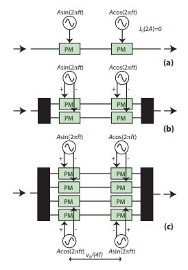
Figure 1. Proposed integrated optical isolators. (a) one-arm, (b)
two-arm, and (c) four-arm designs. PM = phase modulator.
1. Introduction
Integrated optical isolators are needed to isolate lasers and optical amplifiers from back reflections, prevent multi-path interference, and make ring lasers oscillate in one direction. Isolation is especially important when a photonic integrated circuit (PIC) contains lasers or optical amplifiers and is connected to a fiber plant. The traditional method is to use magnetooptic materials [1,2]. However, this generally requires either deposition of polycrystalline films [3], which is challenging due to the large number of elements in garnets, or bonding of crystals [4,5], which is challenging to do on a wafer scale. Most of the demonstrations of integrated isolators that use magneto-optic materials have used ring resonators and thus are narrow band. Also, integrated magneto-optic solutions usually work only for transverse-magnetic polarized light, whereas most PICs work primarily with transverse-electric polarized light. They also usually require placing a magnet on the PIC.
A very different approach is to use electro-optic modulation. It can be integrated in a PIC without needing any special materials or processing steps. One electro-optic method is to employ travelingwave modulators, which give a different modulation depending on the direction of optical propagation. Such designs have either a high intrinsic loss and residual frequency shift [6] or require long modulated sections [7]. Another electro-optic method is to use a tandem arrangement of two phase modulators [8]. This can have low insertion loss and requires only two short modulators. However, it is narrow band.
2. Proposed isolator design
Our proposed improved isolator design is based on the tandem phase modulator scheme shown in Fig. 1(a). In the basic tandem phase modulator scheme, one modulator is driven by a sine wave at frequency f , and the other by a cosine wave also at frequency f . The two phase modulators in each pair are separated by a waveguide propagation distance of vg/(4 f), where vg is the optical group velocity in the waveguides. When the signal passes from left to right in the top arm, the transmission is
ejAsin[2πf(tΔT)]ejAcos(2πft), (1)
where ΔT is the time delay between phase modulators and is equal to 1/(4 f). When the signal passes from right to left, the amplitude transmission is
ejAcos[2πf(t-ΔT)]ejAsin(2πft), (2)
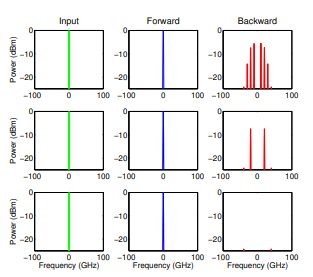
Figure 2. Simulated performance of the isolator designs using a cw
input. The rows show results for the one-arm, two-arm, and four-arm
designs, respectively. f = 10 GHz
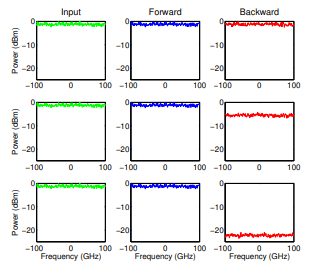
Figure 3. Simulated performance of the isolator designs using a
broadband input. The rows show results for the one-arm, two-arm, and
four-arm designs, respectively. f = 10 GHz.
Eq. 1 is equal to 1, and Eq. 2 is equal to ej2Asin(2πft).
Thus there is no effect on the forward signal, and when J0(2A) = 0 (peak-to-peak modulation of 138°) the carrier is fully depleted from the backward signal, and all the backward energy appears at other wavelengths. This can be seen in the simulated performance shown in the top row of Fig. 2.
The problem with this design is that the isolation is narrow band. The backwards propagating light is distributed to other frequencies, and thus if a broadband input is applied to this device, no isolation is observed, as shown in the top row of Fig. 3.
Our proposed new design is shown in Figs. 1 (b) and (c). It comprises placing one of the abovedescribed narrow-band isolator in each arm of a Narm interferometer. The N narrow-band isolators are identical except that each is driven with a different overall RF phase. The relative RF phase in arm n is 2π(n 1)/N. The optical phase is equal in all arms. In the forward direction, there is no effect on the signal from each narrow-band isolator, and thus the final combined signal also experiences no effect and 100% transmission. In the backward direction, however, because each narrow-band isolator is driven with a different overall RF phase, the generated sidebands interfere destructively, and thus there is broadband isolation. The broadband isolation can be seen in the simulations in the 2nd and 3rd rows of Fig. 3. The larger N is, the higher the isolation. To facilitate implementation, one would like f to be as low as possible. This can be done by lengthening the waveguide propagation distance between the two modulators, vg/(4 f). Regardless of how low f is, the isolation will remain broadband.
3. Experimental demonstration
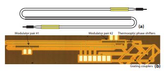
Figure 4. (a) Schematic and (b) photograph of the optical isolator in silicon photonics. The schematic does not show the grating coupler portion.
To test the basic principle, we made a two-arm version in silicon photonics. A schematic and photograph of the device are shown in Fig. 4. There are two pairs of push-pull current-injection plasma-effect modulators in a two-arm interferometer. The modulators are 600 µm long. The width of the intrinsic layer is 1.75 µm.
Each push-pull pair is connected n to n in series with a bias control connected to the n terminals. The waveguide length between the modulator pairs is 7.8 mm, and thus the ideal modulation frequency is 2.4 GHz.
There is a thermooptic phase shifter to control the relative phase in the long interferometer. The input/output coupling to the PIC is via two 1-D grating couplers. We aligned a fiber assembly to the PIC to couple light in and out of the isolator. We drove each modulator pair with a 50-W ground-signal probe. The bias voltage was -0.5V. The modulator bandwidth was 300 MHz. Because of the low bandwidth, the modulator response at 2.4 GHz was weak. To compensate, we drove the modulators at 2.0 GHz at 10V peak-to-peak. Despite this, the peak-to-peak modulation was significantly less than the desired 138, limiting the achievable isolation.
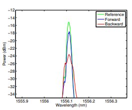
Figure 5. Measured performance of the isolator with a cw laser input. The reference is taken with the modulators turned off.
We first launched a cw laser through the device. The fiber-to-fiber insertion loss at 1550 nm was 11.1 dB. The estimated loss breakdown is the following: 7 dB from fiber coupling in and out, 2 dB waveguide propagation loss, 1 dB from the 1 ⇥ 2 multimode interference couplers, and 1 dB from the two modulators. We drove both modulator pairs with 2.0-GHz sine waves. We adjusted the RF phase between the drives such that in the forward direction there was no effect on the laser signal, and we adjusted the optical phase between the interferometer arms for maximum forward transmission. We swapped the input and output connections (without readjustment of the RF and optical phases) to measure the backward signal. The measured performance for the cw laser input is shown in Fig. 5 using an optical spectrum analyzer. The spectrum analyzer cannot fully resolve the 2-GHz features, but one can see that the narrow-band isolation is ⇠5 dB, limited by insufficient modulation amplitude. The signal when the modulation is turned off is ⇠3 dB higher than the forward direction. This loss is due to residual amplitude modulation due to free-carrier absorption that accompanies the phase modulation, which also limits the achievable isolation.
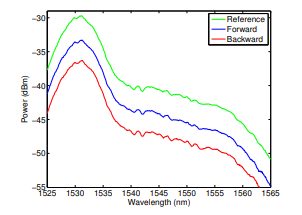
Figure 6. Measured performance of the isolator with amplified spontaneous emission input. The reference is taken with the modulators turned off.
We then launched amplified spontaneous emission from an Er-doped fiber amplifier into the device. The measured spectra are shown in Fig. 6. 3.0 dB of isolation over the C-band was achieved. While this isolation is less than the theoretical value of 6 dB for a two-arm design, it does prove the principle and can be improved significantly by using a four-arm design.
In conclusion, we proposed and demonstrated a novel broadband integrated optical isolator. It can use low modulation speeds, does not require any special materials or fabrication, and has low intrinsic insertion loss. We achieved 3 dB of broadband isolation. The main limitations in the isolation were low modulator bandwidth and using only two interferometer arms. We acknowledge S. Stulz, X.-M. Xu, T. Nielsen, S. Azemati, G. McBrien, B. Mikkelsen, and C. Rasmussen for their support and discussions.
References
- M. Levy, J. R.M. Osgood, H. Hegde, F. J. Cadieu, R. Wolfe, and V. J. Fratello, IEEE Photon. Tech. Lett. 8,
903 (1996). - H. Shimizu and Y. Nakano, IEEE Photon. Tech. Lett. 19, 1973 (2007).
- L. Bi, J. Hu, P. Jiang, D. Kim, G. Dionne, L. Kimerling, and C. Ross, Nature Photonics 5, 1 (2011).
- Y. Shoji, T. Mizumoto, H. Yokoi, I.-W. Hseih, and R. Osgood, Applied Physics Letters 92, 071117 (2008).
- M. Tien, T. Mizumoto, P. Pintus, H. Kroemer, and J. Bowers, Optics Express 19, 11740 (2011).
- S. Bhandare, S. K. Ibrahim, D. Sandel, H. Zhang, F. Wust, and R. Noe, IEEE J. Sel. Topics Quantum Electron. 11, 417 (2005).
- Z. Yu and S. Fan, Nature Photonics pp. 91–94 (2009).
- C. R. Doerr, N. Dupuis, and L. Zhang, Opt. Lett. 36, 4293 (2011).
