In the beginning
Innovation is in our DNA and at the core of what we do every day. Our founders recognized a market opportunity leveraging silicon photonics and, as a result, built a new kind of technology company. Acacia Communications has demonstrated a rapid pace of innovation by taking calculated risks while being pragmatic. We have assembled a team of cross-functional experts capable of solving the challenges of next generation optical interconnects. As we celebrate the debut of this blog, I’d like to look back to share our story and some of the characteristics that make Acacia unique.
Just before 2000, investors and entrepreneurs were focused on the promise of the Internet – primarily, how they could sell more goods and services to consumers on this exciting medium. Many companies in Massachusetts continued to do what they do best – solving the critical, less glamorous but difficult technology problems that helped build the foundation of the internet.
It was a hotbed for networking technology … until it wasn’t. As investors fled online companies, they also abandoned the underlying technologies that allowed them to do business. For the next ten years, the networking hardware sector had seen vast underinvestment—and ultimately, billions of dollars of market cap, gone.
Following the crash of the dot com bubble and the Great Recession in 2007 and 2008, investors were hesitant to invest in the promise of networking technology. Yet our founders, Mehrdad Givehchi, Benny P. Mikkelsen, and Christian J. Rasmussen saw an opportunity in 2009 to combine the processing power of silicon based integrated circuits with emerging silicon photonics technology.
As communications networks increasingly relied on content from “the cloud,” major data centers and carriers were delivering more content than ever, to consumers and businesses alike. End-users expected their information in an instant – and would look elsewhere when they didn’t get it. Cloud and service providers needed innovation to enable the geographic scale of the cloud and cost effectively utilize the fiber optic investments they had made.
I joined the company in early 2010 and built out other functions to commercialize these developments. Together, we formed a team with a wide range of expertise in signal processing, optics, hardware and software design, as well as operational execution. As optical interconnects needed more advanced signal processing, this was exactly the kind of team needed for success.
So What Were We Building Here Exactly?
(Trust me; we’ll keep this pretty high level.)
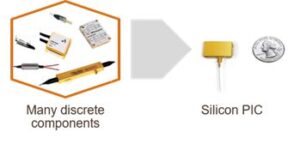
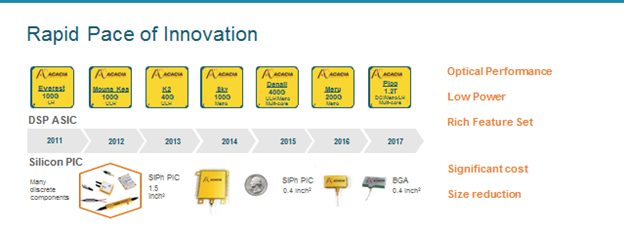
When Acacia started, almost every element of a high-speed network was based on silicon technology — except for one: the optical interconnects that link all the network elements together. Think of the Interstate Highway system, but instead of traversing from I-90 to I-87 through a cloverleaf, you’d do so on a gravel road. Our idea was to replace the exotic materials typically used for optical interconnects with silicon, leveraging the benefits and scale of standard CMOS processes. Interconnects went from the size of a pizza box to the size of a quarter – requiring a smaller footprint AND significantly reduced power.

Our first product, introduced in 2011, demonstrated our ability to produce high performance optical interconnect solutions that address the needs of content and communication network providers and we have been innovating ever since.

We’ll share more about our current products, industry trends and focus on the future in upcoming articles. Stay tuned!
Hello Wall Street!
2016 was an exciting and successful year for Acacia, from completing our IPO in May to doubling our revenues and nearly quadrupling our non-GAAP net income.
We’ve come a long way in these eight years. This is exciting stuff – and solving these challenges while addressing new ones is what makes me eager to get to the office each morning.
Today, we’re helping more than 25 cloud and service provider customers meet the fast-growing corporate and consumer demands for data and online content. These companies are choosing siliconized optics to make this happen. With the emergence of 5G networks and the ubiquity of the Internet of Things, the future and its possibilities are coming at the speed of light.
Yet despite these achievements, Acacia doesn’t stray far from its roots, built on a foundation of fiscal responsibility, innovation and social responsibility:
- We have a beautiful, newly expanded corporate headquarters in Maynard, MA housing new office and lab space in a historic brick and beam building.
- We’re investing in expanding our research, development and manufacturing capabilities – getting the “best people on the bus,” through a rigorous selection process that has allowed us to add to our amazingly talented, experienced team.
- We are active in the communities we call home. The Acacia Community Charter is committed to Science, Technology, Engineering and Math (STEM) related public educational efforts as well as supporting our employees’ commitment to causes that are important to them, supporting matching gifts and one paid volunteer day per calendar year for employees who wish to donate their time.
It’s been fun to look back. But it’s exciting to look ahead, and ultimately, it’s time to get back to work. The next generation of silicon optical interconnects aren’t going to build themselves.
If you have topics you’d like to hear about from Acacia, contact us. We welcome your feedback!
