It’s no secret that silicon photonics has driven significant reductions in the power, size and cost of optical modules. If you look around the telecom industry today, you will see that an increasing number of optics vendors are leveraging this technology for their pluggable coherent solutions. However, this was not always the case. If you looked back 9 years ago, you would see that many companies were challenging whether silicon photonics was even going to work at 100G coherent optics.
Acacia was a pioneer of silicon photonics in 2012 when it was the first coherent module vendor to envision silicon as the platform for the integration of multiple discreet photonic functions while increasing the density and reducing cost of optical interconnect products. According to Gazettabyte, Acacia’s choice to back silicon photonics for coherent optics was an “industry trailblazing decision.”
Leveraging advancements in silicon photonics processing, Acacia was able to deliver generations of high-volume silicon photonics-based products that continually enabled higher transmission data rates, lower power, and higher performance than the generation before it. Early on, some skeptics dismissed silicon photonics as incapable of achieving the performance required for coherent optical transmissions over long-haul distances. As evidenced by today’s deployments of Acacia’s 1.2T multi-haul AC1200 coherent optical module in well over a hundred customer networks which include subsea, long-haul, regional, metro and DCI applications, it is clear that silicon photonics can achieve industry leading performance.
Today, Acacia’s solutions leveraging silicon photonics are available in a wide range of coherent optical interfaces, from edge and access to subsea applications, to enable high-speed transmission and excellent performance.

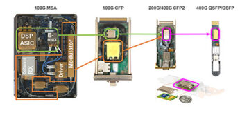
Acacia’s silicon photonics leadership timeline for coherent transmission.
The Power of Silicon Photonics
Using silicon as an optical medium and leveraging CMOS fabrication processing technology, silicon photonics allows tighter monolithic integration of many optical functions within a single device. While traditional optics systems used many discrete pieces, silicon photonics allows all those pieces to fit onto a single silicon chip. This tight integration is what has allowed component vendors to continually drive reductions in the cost and size of optical solutions. For network equipment manufacturer customers, using the silicon photonics chip means they can design more ports per linecard, increasing the capacity of their system.
Below are a few reasons that silicon photonics has been so successful and has emerged as a key technology for existing and future optics solutions.
- Leverages CMOS Processes– Silicon photonics leverages the higher yields and lower cost associated with CMOS. Leveraging mature silicon process technologies means that much larger wafers can be made in silicon than traditional optics materials. Today’s silicon photonics solutions run on lines that accommodate up to 12-inch wafers or larger. These larger wafers result in an order of magnitude more dies per wafer, which lowers cost.
- Enables Package Level Integration – As the industry continues to move toward higher data rates and lower power, the interface between the DSP and high-speed optics is quickly becoming a bottleneck. Every time a high-speed signal needs to transition across an additional electrical interface (solder bumps, wire-bonds, vias, PCB traces) there is loss and distortion. Compensating for this additional loss adds power dissipation, and distortion limits performance. Using silicon photonics enables package-level integration that can better optimize these high-speed interfaces and accelerate the realization of higher data rates at lower power. In addition, silicon photonics is temperature tolerant and thus is not affected by the heat-generating DSP.
- Ensures High Reliability –
- Overall, silicon photonics increases reliability with the high level of integration reducing the number of component interconnects, which are a common source of failure
- Traditional optics degrade in high-moisture environments, requiring optics to be packaged in costly hermetic gold boxes, which are historically one of the most common sources of failure for optics. Silicon, on the other hand, does not require hermiticity so by using silicon photonics the costly gold boxes are eliminated which improves reliability
- In addition to having higher yields than traditional optics materials, silicon photonics can also be tested at the wafer level. Good die can be identified early in the process, and there is no labor wasted on material that will ultimately fail thereby reducing cost.
- Simplifies Deployment and Management – Pluggable modules with industry standard interfaces allow vendors to simplify their networks.
Higher baud rate designs
The next battle for the industry is achieving higher baud rates in a cost-effective way. As the gap to Shannon’s Limit narrows, it is becoming more difficult to increase channel capacity by increasing the modulation order while keeping the same transmission distance. This leaves higher baud rates as a preferred method to increase capacity and decrease cost per bit. Silicon photonics and advances in packaging technology enabled by silicon photonics are key for enabling higher baud rate designs.
Component Stacking
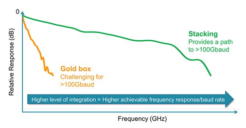
In component stacking, electrical impairments are reduced due to very short electrical connections between key RF components, creating a robust signal path for extremely high frequency/baud rate operation. In this stacked design, the gold-box packaging is eliminated, the DSP, and PIC are tightly co-packaged on the same substrate, and the high-speed modulator driver and TIA components are stacked on the PIC. Stacked design has a higher (better) frequency response than the traditional gold-box design. Advanced stacking designs can further reduce interconnect impairments, resulting in even higher frequency response.

Illustration of example electrical interconnect frequency response comparing traditional gold-box and stacking integration shows that stacking provides a path to >100Gbaud.
New, Innovative Architectures and Future Innovations
Because of its ability to drive performance and volume manufacturability, silicon photonics has the potential to unlock new architectures needed to keep up with rising demand. An example is pluggable coherent transceivers that can be plugged directly into switches and routers offering the same density for both coherent DWDM and client optics in the same chassis. It can also drive future generations of optics design that push the envelope on performance, cost, complexity, and size.
The industry is now turning to silicon to produce a wide variety of devices, using mainstream silicon manufacturing process technologies that have matured over many years. As optical transceivers need to support higher data-rate, driven by the demand for higher speed networks that can handle the rising bandwidth demand, we believe silicon photonics will once again allow the capacity to grow without significantly increasing the size and cost of the devices needed for the future. For this reason and the benefits discussed above, Acacia plans to use silicon photonics in all coherent applications going forward to help customers stay ahead of the curve.


