Increasing Capacity While Reducing Power and Size
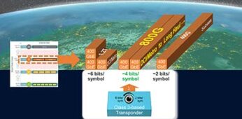
Over the last 10 years, we’ve seen rapid increases in capacity per wavelength by increasing modulation order from QPSK to 16QAM to 64QAM, as well as increasing baud rate supported by opto-electronic devices. However, beyond the coherent modulation order of 64QAM, the achievable performance isn’t sufficient to address target applications due to the reduction in reach. As a result, increasing baud rates has been looked to as the primary means of increasing capacity per wavelength. This requires innovative and cost-effective implementations to provide higher baud rate solutions and packaging advancements. Opto-electronic integration and co-packaging are techniques that were discussed by Acacia’s Founder and Chief Technology Officer Benny Mikkelsen in his OFC 2019 Plenary talk and continue to be critical to support the ever-increasing need for higher data rates and smaller, cost-effective optical interfaces for cloud, access, and transport applications.
Opto-Electronic Integration and Co-Packaging Explained
These techniques are used to reduce components in size and power while also increasing functionality and performance of the solution. Opto-electronic integration generally refers to the process of integrating a wide range of optical functions on a single chip, such as the large amount of optical and opto-electronic functions being achieved in a photonic integrated circuit (PIC). While co-packaging is the ability to combine multiple chips into a single package which can be further integrated into a transceiver module. The main benefit is that it can then be manufactured as if it’s a single component with even more functions.
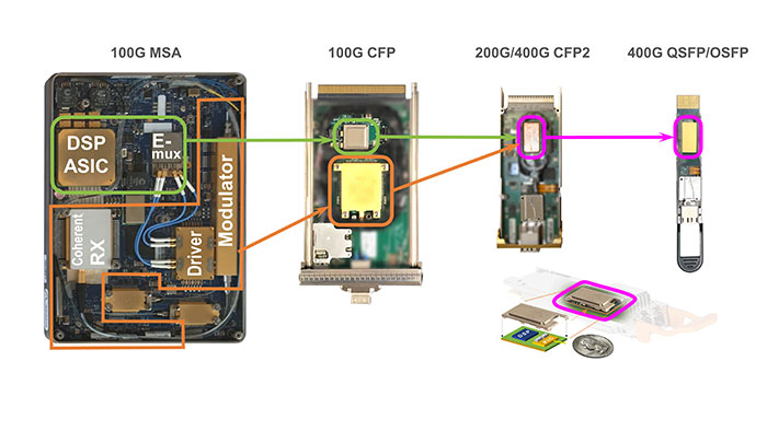
Opto-electronic integration, particularly through silicon photonics, enables the miniaturization of coherent transceivers. The benefits of opto-electronic integration can be seen in the below graphic, which shows how the size of a coherent transceiver was reduced significantly over a few product generations. By leveraging these techniques, each new generation was able to raise the bar to increase capacity while reducing power and size.
Three Main Benefits of Opto-electronic Integration and Co-Packaging
1. Reduced Power
It takes a massive amount of power to operate data centers, which is why sustainability ranks top on data center operator’s agendas. Opto-electronic integration and advanced packaging helps lower the power consumption of the coherent modules used for moving data across networks.
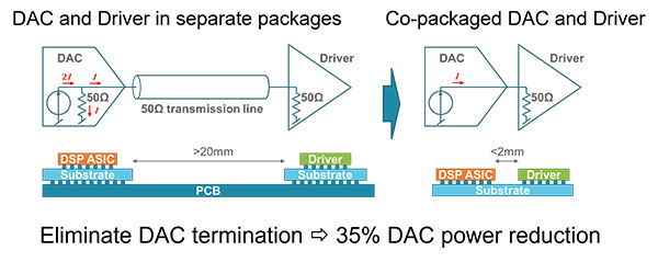
The benefit of having multiple devices packaged into one compact component means fewer interfaces and the ability to support higher speeds per lane. Electrical compensation of PCB routed high-speed signals, which consumes power, is essentially eliminated. As an example, by co-design and co-packaging the trans-impedance amplifier (TIA) and driver chips with the silicon photonics-based PIC on the same substrate as the digital signal processor (DSP) ASIC, the DAC termination can be eliminated and can result in a 35 percent DAC power reduction.
2. Reduced Size
Silicon Photonics
Using silicon as an optical medium and leveraging CMOS fabrication processing technology, silicon photonics allows tighter monolithic integration of many optical functions within a single device. While traditional optics systems used many discrete devices, silicon photonics allows all those devices to fit onto a single silicon chip reducing the size. Silicon photonics has been a key enabler for achieving the tremendous size reduction in Figure 1.
Component Stacking
In component stacking, the DSP and PIC are tightly co-packaged on the same substrate, and the high-speed modulator driver and TIA components are stacked on the PIC which also reduces the size. Component stacking is a process widely adopted in the electronics manufacturing process that is now being applied to opto-electronic technology manufacturing.
Co-packaging and Integrated Control IC
Size reductions are achieved by integrating functions and the control IC through co-packaging techniques. Smaller devices can translate into either more functionality within the same form factor and power consumption footprint or a smaller form factor with the same functionality and power consumption as the previous generation. For example, in the Acacia CFP2 form factor, the integration of multiple discrete control ICs into one integrated device led to a 500 percent reduction in board footprint.
3. Increased Capacity
Enhancing DSP and Increasing Baud Rate
With network capacity demands increasing, network operators are challenged with an ongoing need to deploy solutions that can keep up with these capacity demands while being power, size and cost efficient. High speed opto-electronic integration and advanced packaging can deliver high-capacity transport from the state-of-art DSP.
Increasing baud rate has always been an efficient way to enable more cost-effective optical networks by reducing the number of optics required to support a given transmission capacity. By doubling baud rate over previous generations, we can support twice the capacity per carrier over greater reaches than prior generations. This approach provides a simple, scalable path that supports higher capacity per carrier over the reaches needed for existing and new network architectures.
Acacia’s Implementation: 3D Siliconization
Acacia’s approach to co-packaging is called 3D Siliconization technology. This process utilizes highly scalable and reliable volume electronics manufacturing processes which applies 3D stacking packaging techniques to enable a single device to include all the high speed opto-electronic functions necessary for coherent transceivers. With 3D Siliconization, the high-speed RF interfaces are tightly coupled together, resulting in improved signal integrity for high baud rate signals.
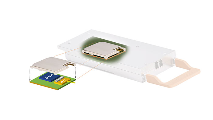
This device decreases footprint by including the DSP, PIC, drivers, and TIAs, and is manufactured using standard CMOS packaging processes that leverage the same reliability, cost, and volume scaling advantages. This approach is utilized by Acacia’s 400G pluggable family and the 1.2T 140Gbaud Coherent Interconnect Module 8 (CIM 8).

